Demartek Comments on FMS2015 and IDF2015
September 2015
By Dennis Martin, Demartek President
In August 2015, I attended the Flash Memory Summit (FMS) and the Intel Developer Forum (IDF), which were only a few days apart.
Flash Memory Summit 2015
 2015 was the tenth anniversary of the Flash Memory Summit, which had an expanded session room area compared to
last year, and the exhibit hall was about 30% larger than last year. Registrations for the event were more than
5200, a 7% increase from 2014, and actual attendance was 4074 people, an increase of 4% over 2014.
Toyota had a big presence at this year’s Flash Memory Summit. They discussed new “intelligent driving technology” features designed to avoid human-error induced incidents and to reduce traffic congestion. These features use flash memory to store and retrieve the necessary data to react quickly to emergency incidents. For example, they are working on risk prediction models and emergency avoidance controls that have the ability to predict the possibility of pedestrians appearing from behind an object such as a parked car and then take appropriate action.
There were many announcements of new products, form factors and types of non-volatile memory. Samsung announced a 16 TB 2.5-inch SSD — not only the largest capacity SSD — but larger than any commercially available hard disk drive. 3D NAND flash was another big item, promising to increase the performance, reliability and capacities of NAND flash devices. 3D NAND is able to do this because it is built in layers in the “vertical” dimension while some of the technical constraints are relaxed compared to planar (2D) NAND. I saw many M.2 form-factor SSDs on display that are designed for small form factor applications, including televisions, laptop computers and others. There were also several new NVMe devices, including 2.5-inch drives, M.2 modules and PCIe cards. I was also glad to see the progress in hybrid and all-flash arrays on display at the show.

Another hot topic was using the memory channel for storage in a form factor known as NVDIMM. This is a combination of DRAM, NAND flash or both on a module that fits into a standard DIMM socket but that can behave as memory, storage or both. There are some interesting implications for programming modules for this type of “persistent memory” for operating systems, file systems and applications. I will write a separate commentary piece on this topic.
There was lots of buzz regarding the new Intel/Micron memory technology. In July 2015, Intel and Micron jointly announced a “breakthrough” new memory technology called 3D XPoint™ (“cross point”) technology. They claim that this “technology is up to 1,000 times faster and has up to 1,000 times greater endurance than NAND, and is 10 times denser than conventional memory.” This certainly has the potential of filling a gap between today’s DRAM and today’s NAND flash memory, and may be complementary to both initially. I sat in the front row of one extremely well-attended session where there was speculation about this new type of memory, and the panelists gave their opinions about the underlying technology for this new memory. There were no representatives from Intel or Micron on the panel or in the room, but there was quite a bit of lively discussion and questions from the packed room of several hundred people. See the Intel Developer Forum commentary below for more details.
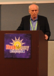 I spoke each day of the Flash Memory Summit 2015, either in panel sessions or my own session. One of my main
themes, which was echoed elsewhere during the show, was that flash storage can handle multiple real-world
workloads. In my session (104-C), I explained the difference between synthetic benchmarks and real-world
applications and their effects on storage devices and external storage systems. I also discussed the difference
between taking performance measurements, especially latency, at the physical host application server, from
within a virtual machine and at the storage system. I gave several examples of multiple workloads running,
including one example of running a collection of web servers, two SQL Server workloads, one Exchange
Jetstress workload and a SharePoint workload simultaneously on a single all-flash array. I also gave a
short presentation at the Storage Valley Supper Club one evening on some of the new interfaces that will
be used for storage devices, such as Ethernet, Fibre Channel, Thunderbolt 3 and others. These presentations
are available on the
Demartek FMS2015 presentation
page.
Intel Developer Forum 2015
Less than a week later, I attended the Intel Developer Forum where one of the main attractions was Intel’s presentation of their new 3D XPoint memory. In the opening keynote address, Intel CEO Brian Krzanich gave a demonstration of this new memory. They brought a server onto the stage with this new memory configured as an SSD and showed it running some performance tests along with another server running the same tests with an Intel NAND flash DC P3700 SSD. The performance meters consistently showed 5 — 7 times faster performance for this new memory running as an SSD in the test workloads compared to a NAND flash SSD.
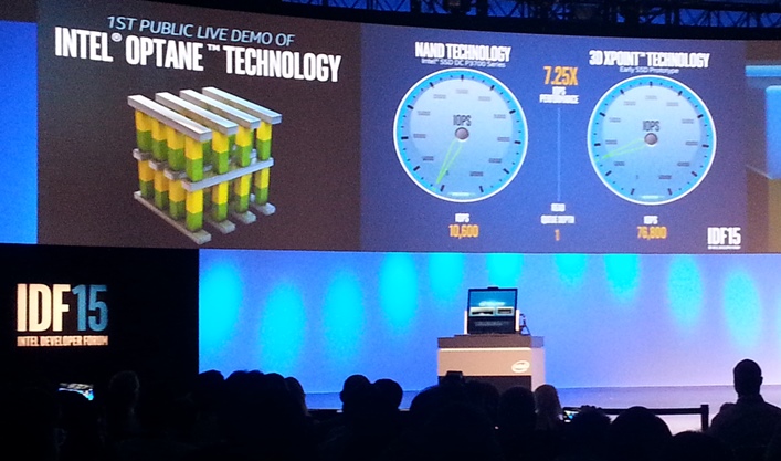
I was told that this was the first time that any of this memory had been taken outside of an Intel or Micron facility. In an analyst briefing immediately following this keynote presentation, Intel answered a few more questions about this memory. They said that they would make it available in DIMM form factor for server memory (with ECC) and as storage in various SSD form factors. They are building it using a 20 nm process and they can build 2D NAND and 3D XPoint in the same fab. They did not describe the underlying physics of this memory other than to say that, unlike NAND flash, it contains no transistors and that it was something new that they had been developing for some time. They said that they expect shipments to begin in 2016 and that they would eventually reveal technical details regarding this memory. There will be much speculation and analysis of the underlying technology of this memory. They also announced “Optane,” which is the platform that includes the controller technology along with the 3D XPoint memory.
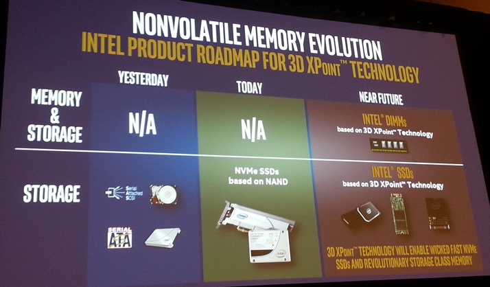
I believe that this may not be the only “breakthrough” memory that is announced over the next few years, but it certainly raises awareness of persistent memory and some of the very interesting hardware and software changes that will affect compute and memory as we know it today.
There were also several sessions devoted to NVMe and a good collection of vendor booths in the NVMe community on the exhibit show floor. It is nice to see more companies providing NVMe devices and the ecosystem maturing. I expect to see some NVMe client devices soon and some progress on the very interesting NVMe over Fabrics technology.
I saw some prototype PCIe gen 4 technology on display in one booth. The PCIe 4.0 specification is currently at version 0.5, with version 0.7 expected by year-end 2015. Revision 0.9 of this specification is expected in 2H 2016. This means that PCIe 4.0 products may be available in 2017 or 2018.
I also spent time discussing Thunderbolt 3 and USB 3.1 in those respective communities, and have posted the latest information about these and other interfaces on our Storage Interface Comparison page.
On the consumer side, there were many new interesting examples of wearable technology and sensor technology on display. They demonstrated a digital fitting-room mirror that lets people see themselves with different colors of clothes virtually and send photos to friends. There were many 3D scanning and plotting applications, and no discusion of IDF2015 would be complete without mentioning the dancing Intel spiderbots.
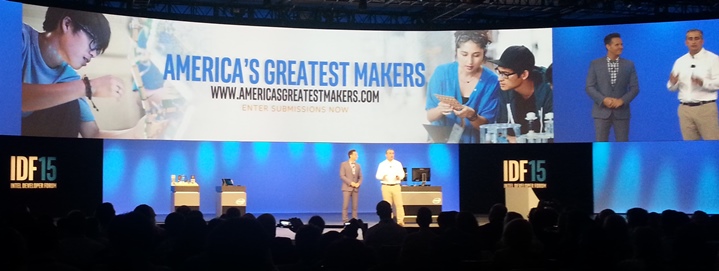
During the main keynote presentation, Intel CEO Brian Krzanich invited Hollywood Producer Mark Burnett (“The Voice”, “Shark Tank” and others) on stage with him to announce a new television show to air in 2016. The working title is “America’s Greatest Makers” and it is a collaboration between Intel, Mark Burnett, United Artists Media Group and Turner Broadcasting System. The goal of this production will be to highlight innovation and new ideas in wearable technology. Entrants must be 15 years of age or older and the competitors will vie for a $1 million dollar prize. The application submission deadline is October 2, 2015. Additional details are available at www.americasgreatestmakers.com.
Other Related Commentaries
- Demartek Discusses 3D NAND, NVMe and NVDIMM
- CES 2016 Comments
- Storage Decisions New York 2015
- Flash Memory Summit 2014 Commentary
- IDF2014: NVMe, Thunderbolt 2, USB 3.1 & PCIe 4.0
Demartek public projects and materials are announced on a variety of social media outlets. These include Facebook, LinkedIn, Twitter and YouTube. Click any of the icons below to visit our pages.


 We are pleased to announce that Principled Technologies has acquired Demartek.